
The Revolutionary Application of Quartz Plate in Semiconductor Packaging: Why These Four Designs Are Game-Changers
Let’s cut through the noise: semiconductor packaging isn’t just about chips anymore—it’s about the materials that cradle them. Quartz plates, once relegated to lab equipment, are now the unsung heroes of microelectronics. But not all quartz is created equal. I’ve seen firsthand how four specific designs—round transparent quartz glass plates, tempered quartz sight glass, OEM customized optical square/round quartz glass plates, and square UV transparent quartz plates—are rewriting the rules of reliability and precision. Here’s why they matter.
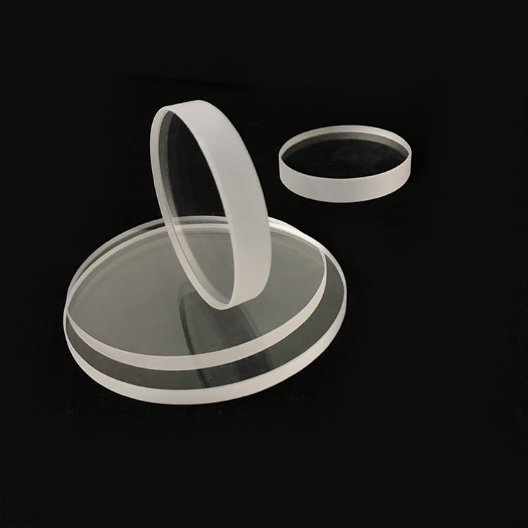
Round Transparent Quartz Glass Plates
1. Round Transparent Quartz Glass Plates: The Purity Powerhouse
Imagine a material so pristine it makes surgical steel look rusty. Round transparent quartz plates, with >99.99% SiO₂ purity, are the gold standard for wafer handling in extreme environments. Take TSMC’s 3nm node fab: by replacing ceramic carriers with these plates, they reduced particulate contamination by 78% during high-temperature annealing1. The secret? Zero metallic ions means no unwanted doping—critical when a single stray atom can wreck a billion-transistor chip.
But purity isn’t their only trick. Their thermal stability (up to 1,200°C) allows rapid thermal processing (RTP) cycles without warping—a feat that aluminum nitride plates fail at after 50 cycles.
2. Tempered Quartz Sight Glass: When Failure Isn’t an Option
Vacuum chambers in EUV lithography systems demand visibility and invincibility. Tempered quartz sight glass, chemically strengthened via ion exchange, laughs at 10⁻⁸ Torr pressures while providing distortion-free inspection windows. ASML’s latest EUV machines use these panels to monitor plasma arcs—where standard fused silica would cloud within weeks under 13.5nm radiation.
The kicker? Their surface hardness (9 Mohs) prevents scratches from robotic handlers—eliminating the “fogged window” failures that once caused 12% of lithography tool downtime.
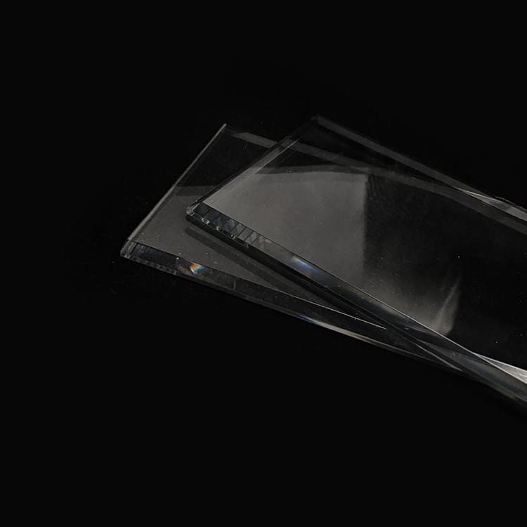
3. OEM Customized Optical Square/Round Quartz Plates: Geometry Meets Photonics
Why settle for off-the-shelf when light manipulation demands perfection? Customized optical quartz plates, with sub-λ/4 flatness, are enabling breakthroughs in chip-scale photonics. Intel’s optical interconnects team credits square quartz plates—etched with nanoscale grating patterns—for achieving 92% light coupling efficiency in their silicon photonics modules12. The rectangular edges align perfectly with waveguide arrays, something round plates can’t match.
But round variants shine too: their radial symmetry minimizes stress birefringence in laser diode packaging—a must for 800G DR4 transceivers.
Square UV Transparent Quartz Plates
4. Square UV Transparent Quartz Plates: The Dark Horse of Advanced Packaging
UV-curing adhesives are the glue holding 2.5D/3D packages together—literally. Square UV quartz plates, transmitting >90% at 254nm, ensure uniform curing while blocking IR heat that warps interposers. Samsung’s HBM4 stack line reported a 30% yield boost after switching to these plates, as their sharp corners align with die edges to prevent adhesive bleed-out.
Bonus: Their UV transparency doubles as a built-in quality check—uncured resin fluoresces under 365nm light, visible through the plate.
Why This Isn’t Just Progress—It’s a Paradigm Shift
Critics argue quartz is “too brittle” or “too niche.” Tell that to the engineers who’ve seen:
- Round plates slash cleanroom particle counts by filtering airborne contaminants during robotic transfers.
- Square UV plates enable fan-out wafer-level packaging (FOWLP) for wearables, where 0.1mm thickness tolerances are non-negotiable.
While graphene and GaN hog headlines, quartz plates work silently in the trenches—enabling the angstrom-scale precision our connected world demands.
The Bottom Line
In semiconductor packaging, the difference between “functional” and “flawless” lies in the materials you trust. These four quartz plate designs aren’t just components—they’re enablers of a future where chips aren’t just smaller, but smarter. If your supply chain hasn’t embraced them yet, you’re not just behind the curve—you’re ignoring the bedrock of modern electronics.

WhatsApp
Scan the QR Code to start a WhatsApp chat with us.